Monday, March 30, 2009

Digital Hall Effect Sensor Connection

The output of a digital Hall effect sensor is NPN (current sinking, open
collector), as shown in Figure 4-1. The illustration shows the outputs
in the actuated (ON) state.

Current sinking derives its name from the fact that it “sinks current from a
load.” The current flows from the load into the sensor. Current sinking
devices contain NPN integrated circuit chips. The physics of chip
architecture and doping are beyond the scope of this book.
Like a mechanical switch, the digital sensor allows current to flow when
turned ON, and blocks current flow when turned OFF. Unlike an ideal
switch, a solid state sensor has a voltage drop when turned ON, and a
small current (leakage) when turned OFF. The sensor will only
switch low level DC voltage (30 VDC max.) at currents of
20 mA or less. In some applications, an output interface may
be current sinking output, NPN.
Figure 4-2 represents an NPN (current sinking) sensor. In
this circuit configuration, the load is generally connected
between the supply voltage and the output terminal
(collector) of the sensor. When the sensor is actuated, turned
ON by a magnetic field, current flows through the load into
the output transistor to ground. The sensor’s supply voltage
(VS) need not be the same value as the load supply (VLS);
however, it is usually convenient to use a single supply. The
sensor’s output voltage is measured between the output terminal
(collector) and ground (-). When the sensor is not
actuated, current will not flow through the output transistor
(except for the small leakage current). The output voltage, in this
condition, will be equal to VLS (neglecting the leakage
current). When the sensor is actuated, the output voltage will drop
to ground potential if the saturation voltage of the output
transistor is neglected. In terms of the output voltage, an NPN
sensor in the OFF condition is considered to be normally
high.

Source pdf
http://www.honeywell-sensor.com.cn/prodinfo/

magnetic_position/technical/chapter4.pdf


ELECTRICAL INTERFACE FOR DIGITAL HALL DEVICES
The output stage of a digital Hall switch is simply an open-collector
npn transistor. The rules for use are the same as those for any similar
switching transistor.
When the transistor is OFF, there is a small output leakage current
(typically a few nanoamperes) that usually can be ignored, and a
maximum (breakdown) output voltage (usually 24 V), which must not
be exceeded.
When the transistor is ON, the output is shorted to the circuit
common. The current flowing through the switch must be externally
limited to less than a maximum value (usually 20 mA) to prevent
damage. The voltage drop across the switch (VCE(sat)) will increase for
higher values of output current. You must make certain this voltage is
compatible with the OFF, or “logic zero,” voltage of the circuit you wish
to control.
Hall devices switch very rapidly, with typical rise and fall times in
the 400 ns range. This is rarely significant, because switching times
are almost universally controlled by much slower mechanical parts.

COMMON INTERFACE CIRCUITS

Figure 17 illustrates a simplified schematic symbol for Hall digital
switches. It will make further explanation easier to follow.
Interface for digital logic integrated circuits usually requires only an
appropriate power supply and pull-up resistor.
With current-sinking logic families, such as DTL or the popular
7400 TTL series (figure 18A), the Hall switch has only to sink one
unitload
of current to the circuit common when it turns ON (1.6 mA maximum
for TTL). In the case of CMOS gates (figure 18B), with the
exception of switching transients, the only current that flows is through
the pull-up resistor (about 0.2 mA in this case).
Loads that require sinking currents up to 20 mA can be drivendirectly

by the Hall switch

A good example is a light-emitting diode (LED) indicator that
requires only a resistor to limit current to an appropriate value. If the
LED drops 1.4 V at a current of 20 mA, the resistor required for use
with a 12 V power supply can be calculated as:

The nearest standard value is 560 , resulting in the circuit of
figure 19.

Source pdf
http://www.allegromicro.com/en/Products/Design/an/an27701.pdf

HALL-EFFECT SWITCHES

Saturday, March 28, 2009

Hall Effect Sensor Direction Sensor

Two digital output Hall effect devices may be used in combination

to determine the direction of rotation of a ring magnet, as shown

in Figure 4-20. The sensors are located close together along the

circumference of the ring magnet. If the magnet is rotating in the

direction shown (counter-clockwise) the time for the south pole of

the magnet to pass from sensor T2 to T1 will be shorter than the

time to complete one revolution. If the ring magnet’s direction is

reversed, the time it takes the south pole to pass from T2 to T1 will

be almost as long as the time for an entire revolution. By comparing

the time between actuations of sensors T2 and T1 with the time for

an entire revolution (successive actuations of T2), the direction can

be determined. A method by which these two times can be compared

is also shown in Figure 4- 20. An oscillator is used to generate

timing pulses. The counter adds these pulses (counts up) starting

when sensor T2 is actuated and stopping when sensor T1 is actuated.

The counter then subtracts pulses (counts down) for the remainder

of the revolution. The shorter time interval between T2 and T1

actuation will result in fewer pulses being added than subtracted,

thus actuating the counter’s BR (borrow) output. When the time

between T2 and T1 is longer, more pulses are added than subtracted

and the BR output is not actuated. For the configuration shown, there

will be no output for clockwise motion and a pulse output for each

revolution for counterclockwise motion. In addition to the interface

design concepts covered in this section, there are many other possible

ways to utilize the output of digital Hall effect sensors. For example,

the output could be coupled to a tone encoder in speed detection

applications or a one-shot in current sensing applications. To a large

extent, the interface used is dependent on the application and the

number of possible interface circuits is as large as the number of

applications.

Figure 4-20 Digital output sensor direction sensor

Source pdf

http://www.honeywell-sensor.com.cn/prodinfo/magnetic_position/

technical/chapter4.pdf

ROTARY ACTIVATORS FOR HALL SWITCHES

A frequent application involves the use of Hall switches to generate

a digital output proportional to velocity, displacement, or position of a

rotating shaft. The activating magnetic field for rotary applications can

be supplied in either of two ways:

MAGNETIC ROTOR ASSEMBLY

The activating magnet(s) are fixed on the shaft and the stationary

Hall switch is activated with each pass of a magnetic south pole

(figure 22A). If several activations per revolution are required, rotors

can sometimes be made inexpensively by molding or cutting plastic or

rubber magnetic material. Ring magnets can also be used. Ring

magnets are commercially available disc-shaped magnets with poles

spaced around the circumference. They will operate Hall switches

dependably and at reasonable costs.

Ring magnets do have limitations:

The accuracy of pole placement (usually within 2 or 3 degrees).

Uniformity of pole strength ( 5%, or worse).

These limitations must be considered in applications requiring

precision switching.

FERROUS VANE ROTOR ASSEMBLY

Both the Hall switch and the magnet are stationary (figure 22B); the

rotor interrupts and shunts the flux with the passing of each ferrous

vane.

Vane switches tend to be a little more expensive than ring magnets,

but because the dimensions and configuration of the ferrous vanes can

be carefully controlled, they are often used in applications requiring

precise switching or duty cycle control.

Properly designed vane switches can have very steep flux density

curves, yielding precise and stable switching action over a wide

temperature range.

Source pdf

http://www.allegromicro.com/en/Products/Design/an/an27701.pdf

Hall Effect Sensor

Hall Sensors Device

Tuesday, March 24, 2009

Hall effect sensor Transfer function

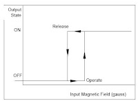
The transfer function for a digital output Hall effect sensor incorporating
hysteresis is shown in Figure 2-11.


Figure 2-11 Transfer function hysteresis Digital output sensor


The principal input/output characteristics are the operate point,
release point and the difference between the two or differential.
As the magnetic field is increased, no change in the sensor output
will occur until the operate point is reached. Once the
operate point is reached, the sensor will change state. Further
increases in magnetic input beyond the operate point will have
no effect. If magnetic field is decreased to below the operate
point, the output will remain the same until the release point
is reached. At this point, the sensor’s output will return to
its original state (OFF). The purpose of the differential between
the operate and release point (hysteresis) is to
eliminate false triggering which can be caused by minor
variations in input.

As with analog output Hall effect sensors, an output transistor
is added to increase application flexibility. This
output transistor is typically NPN (current sinking). See
Figure 2-12. The features and benefits are examined in detail
in Chapter 4.


Figure 2-12 NPN (Current sinking) . . . Digital output sensor

The fundamental characteristics relating to digital output
sensors have been presented. The specifications and the
effect these specifications have on product selection follows.

Source ( pdf )
Honeywel

http://content.honeywell.com/sensing/prodinfo/solidstate/technical/hallbook.pdf

Sunday, March 22, 2009

HALL-EFFECT SWITCHES


The addition of a Schmitt-trigger threshold detector with built-in
hysteresis, as shown in figure 6, gives the Hall-effect circuit digital
output capabilities. When the applied magnetic flux density exceeds a
certain limit, the trigger provides a clean transition from OFF to ON
without contact bounce. Built-in hysteresis eliminates oscillation
(spurious switching of the output) by introducing a magnetic dead zone
in which switch action is disabled after the threshold value is passed.

An open-collector NPN output transistor added to the circuit (figure
7) gives the switch digital logic compatibility. The transistor is a
saturated switch that shorts the output terminal to ground wherever the
applied flux density is higher than the ON trip point of the device. The
switch is compatible with all digital families. The output transistor can
sink enough current to directly drive many loads, including relays,
triacs, SCRs, LEDs, and lamps.

The circuit elements in figure 7, fabricated on a monolithic silicon
chip and encapsulated in a small epoxy or ceramic package, are
common to all Hall-effect digital switches. Differences between device
types are generally found in specifications such as magnetic parameters,
operating temperature ranges, and temperature coefficients.

OPERATION
All Hall-effect devices are activated by a magnetic field. A mount
for the the devices, and electrical connections, must be provided;
Parameters such as load current, environmental conditions, and supply
voltage must fall within the specific limits shown in the appropriate
documentation.


Magnetic fields have two important characteristics—flux density
and polarity (or orientation). In the absence of any magnetic field,
most Hall-effect digital switches are designed to be OFF (open circuit
at output). They will turn ON only if subjected to a magnetic field that
has both sufficient density and the correct orientation.
Hall switches have an active area that is closer to one face of the
package (the face with the lettering, the branded face). To operate the
switch, the magnetic flux lines must be perpendicular to this face of the
package, and must have the correct polarity. If an approaching south
pole would cause switching action, a north pole would have no effect.
In practice, a close approach to the branded face of a Hall switch by
the south pole of a small permanent magnet will cause the output
transistor to turn ON (figure 8).

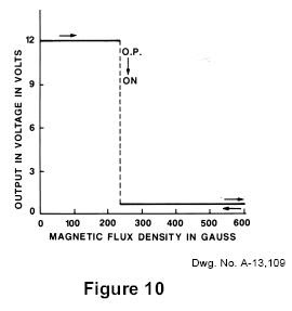
A Transfer Characteristics Graph (figures 10 and 11) plots this
information. It is a graph of output as a function of magnetic flux
density (measured in gauss; 1 G = 0.1 mT) presented to the Hall cell.
The magnetic flux density is shown on the horizontal axis. The digital
output of the Hall switch is shown along the vertical axis.


To acquire data for this graph, add a power supply and a pull-up
resistor that will limit current through the output transistor and enable
the value of the output voltage to approach zero (figure 9).
In the absence of an applied magnetic field (0 G), the switch is
OFF, and the output voltage equals the power supply (12 V).


A permanent magnet’s south pole is then moved perpendicularly
toward the active area of the device. As the magnet’s south pole
approaches the branded face of the switch, the Hall cell is exposed to
increasing magnetic flux density. At some point (240 G in this case),
the output transistor turns ON and the output voltage approaches zero
(figure 10). That value of flux density is called the operate point. If we
continue to increase the field’s strength, say to 600 G, nothing more
happens. The switch turns ON once and stays ON.


To turn the switch OFF, the magnetic flux density must fall to a
value far lower than the 240 G “operate point” because of the built-in
hysteresis. For this example we use 90 G hysteresis, which means the
device turns OFF when flux density decreases to 150 G (figure 11).
That value of flux density is called the “release point”.
Allegro Microsystems inc.
Source ( pdf )
http://www.allegromicro.com/en/Products/Design/an/an27701.pdf

Hall Sensors Device

Bell Technologies Inc.,

1. Hall Sensors Device - Instrumentation Quality

2.
Hall Sensors Device - Single Axis

3. Hall Sensors Device - Three Axis

4.
Hall Sensors Device - High Linearity

Hall Sensors Device - High Linearity

Bulk Indium BH-900 Series
High Linearity


Bell Technologies Inc.,

Description
F.W. Bell 900 Series Hall Sensors are high-performance units
providing high linearity and broad field and temperatures ranges
for a wide variety of magnetic field measurements. All units in the
series are encapsulated in rugged, epoxy, sealed cases.

A room temperature linearity error curve from -30 to +30 kG is
supplied, indicating optimum operating conditions for each device.

The models 900 and 921 are not calibrated above 30 kG.

Models
a. BH-910 High Linearity
b. BH-921 Cryogenic Operation (1.5 to 350° k)
c. BH 921 & 900 Wide Dynamic Range


Hall Sensors Device - Three Axis


Bulk Indium Arsenide BH-703
Three Axis


Bell Technologies Inc.,

Description
The BH-703 multi-axis Hall sensor consists of three individual

Hall elements oriented in mutually perpendicular planes and
encapsulated in a small epoxy package. This enables the BH-703
to produce voltages proportional to the three orthogonal
components (Bx, By, Bz) of a magnetic flux in any direction.

Thus the BH-703 may be permanently mounted or arbitrarily
oriented to sense fields in any direction.

The magnitude of the flux vector, B, can be found using the following
relation:


Features
• Three Axis, simultaneous measurement
• Instrumentation Quality


Hall Sensors Device - Single Axis


Bulk Indium Arsenide BH-700 Series

Single Axis

Bell Technologies Inc.,

Description
Designed to meet the requirements of a wide range of magnetic
field measurement applications, the BH-700 Series are small,
solid-state devices that provide an output voltage proportional to
the product of control current and ambient flux density. Five
single-axis models are available to measure axial and transverse
magnetic field components with sensitivities from 7.5 to 50
mV/kG and input and output resistance of several ohms.

Electrical Specifications

BH-702
a. Air gap: between concentrator and substrate, 0.0025" nominal
and 0.003" maximum.

b. Sensitivity: Basic sensitivity of Hall element .15 V/A-kG min.
With the unit suspended in a free field of 100 oersteds and
Ic=200 mA, the open circuit Hall voltage is 8.0 mV min. In a
closed magnetic circuit with Ic=200 mA, VH is 3.mV/Ampere
turn min.

c. Polarity: With the magnetic field vector as shown and Ic entering
the red lead, the positive Hall voltage will appear at the blue lead.

BH-701
a. Linearity: VH vs. B, –10 to +10 kG: ±0.25% of reading, max.

BH-704
VH vs. B, –30 to +30 kG: ±1.0% of reading, max.
VH vs. Ic, 0 to 100 mA: ±0.1% of reading, max.
VH vs. Ic, 0 to 300 mA: ±1.0% of reading, max.

b. Encapsulation:
The BH-701 and the BH-704 are encapsulated in a rugged aluminum
oxide ceramic and epoxy case for excellent heat transfer and strength.

Models
1. BH-700 Low cost, Transverse, General Purpose
2. BH-701 Rugged, High-Linearity, Transverse, Instrumentation Quality
3. BH-702 Low Field (ferrite-embedded), Transverse
4. BH-704 Rugged, High Linearity, Axial, Instrumentation Quality
5. BH-705 General Purpose, Transverse


Hall Sensors Device - Instrumentation Quality

Bulk Indium Arsenide BH-200 Series

Bell Technologies Inc.,

Instrumentation Quality


Description
The BH-200 series of Hall effect magnetic field sensors consists

of ten models designed to meet the requirements of most
magnetic field measurement applications. Models in the BH-200

Series are built in various configurations to measure axial,
transverse, and tangential magnetic field components. Sensitivities

range from 6 to 75 mV/kG with input and output resistance
of several ohms.


Models
1. BH-200 General Purpose Transverse
2. BH-201 Ultra-thin, Transverse
3. BH-202 Small Axial
4. BH-203 General Purpose, Axial
5. BH-204 Mini Axial
6. BH-205 Mini Transverse
7. BH-206 High Sensitivity, Low-cost Transverse
8. BH-207 High Resolution, Tangential
9. BH-208 Ultra-mini, Axial
10. BH-209 Ultra-mini, Transverse


Saturday, March 21, 2009

Hall Effect Sensor

Hall Effect

Hall Effect

How the Hall effect works

Why use the Hall effect?

Hall Voltage versus Varying Current


Hall Sensor

What Is A Hall Sensor?

Basic Hall Sensor

Hall sensor Typical Shapes and Sizes

Hall sensor Typical Applications

HALL-EFFECT SWITCHES

Hall effect sensor Transfer function


Hall sensor Typical Applications


The following are just some of
the many applications where Hall
Sensors are used:

• Magnetic Card Readers
• Proximity Sensors
• Rotary Speed Sensors
• Watt Measurement
• Multipliers
• Magnet Field Measurements
• Electrical Power Measurements
• Current Sensors
• Brushless dc Motors
• Compasses
• Gaussmeters
• Watt-hour Meters
• Permanent Magnet Measurements
• Air Gap Measurements
• Magnetic Circuit design
• Flux Leakage Measurements
• Nondestructive Memory Readouts
• Linear/Angular Transducers
• Magnetic Tape Heads
• Guidance Systems
• Ignition Systems


Source ( pdf )
Bell Technologies Inc.,

http://www.physics.brown.edu/physics/demopages/
Demo/em/demo/halleffect.pdf

Hall sensor Typical Shapes and Sizes

Bell Technologies Inc.,

Hall sensors are available in a wide variety of shapes and sizes
For adaptability of shapes and sizes for adaptability to many
different applications. The two basic types are transverse and
axial, as illustrated in Figure 4.


The transverse type is useful where the field must be measured in
thin gaps and for multiplier applications. The axial type must be
used where the field is parallel to the axis of a hole, such as in
traveling wave tubes or solenoids. Standard transverse probes as
thin as .006" and axial probes as small as .063" in diameter are
available. Bulk-material Hall plates may be sandwiched between
ferrite pieces to obtain effective air gaps less than .003". This may
be useful in applications requiring maximum magnetic efficiency,
such as electronic compasses and proximity sensors. For a Hall
sensor to accurately measure flux density, the Hall plate area
should be smaller than the cross section of the field to be measured.
The output voltage is proportional to flux density, but a Hall plate is
not equally sensitive over its entire area. If a high resolution is
important, the Hall plate area should be small. Active areas as
small 0.010” are available, while even smaller ones have been made.


Source ( pdf )
http://www.physics.brown.edu/physics/demopages/Demo/
em/demo/halleffect.pdf/

Basic Hall effect sensors

The Hall element is the basic magnetic field sensor.
It requires signal conditioning to make the output
usable for most applications. The signal conditioning
electronics needed are an amplifier stage and temperature
compensation. Voltage regulation is needed
when operating from an unregulated supply. Figure
2-4 illustrates a basic Hall effect sensor.
If the Hall voltage is measured when no magnetic
field is present, the output is zero (see Figure 2-1).
However, if voltage at each output terminal is measured
with respect to ground, a non-zero voltage will
appear. This is the common mode voltage (CMV),
and is the same at each output terminal. It is the potential
difference that is zero. The amplifier shown in
Figure 2-4 must be a differential amplifier so as to
amplify only the potential difference – the Hall voltage.
The Hall voltage is a low-level signal on the order of
30 microvolts in the presence of a one gauss magnetic
field. This low-level output requires an amplifier with
low noise, high input impedance and moderate gain.


A differential amplifier with these characteristics can be readily
integrated with the Hall element using standard bipolar transistor
technology. Temperature compensation is also easily integrated.

As was shown by equation 2-1, the Hall voltage is a function of the
input current. The purpose of the regulator in Figure 2-4 is to hold
this current constant so that the output of the sensor only reflects
the intensity of the magnetic field. As many systems have a
regulated supply available, some Hall effect sensors may not
include an internal regulator.

Source ( pdf )
http://content.honeywell.com/sensing/prodinfo/solidstate/
technical/hallbook.pdf

What Is A Hall Sensor?


Bell Technologies Inc.,

A Hall sensor is a four-terminal, solid-state device capable of
producing an output voltage VH, proportional to the product of the
input current, lc,the magnetic flux density, B, and the sine of the
angle betweeen B and the plane of the Hall sensor. A reversal in
the direction of either the magnetic field or the control current will
result in a polarity change of VH. A reversal in the direction of
both will keep the polarity the same. By holding the control current
constant, the Hall voltage may be used to measure magnetic flux
density. Multiplication may be accomplish by varying both the
control current and the magnetic field..


Source ( pdf )
http://www.physics.brown.edu/physics/demopages/Demo/
em/demo/halleffect.pdf

Hall Voltage versus Varying Current

Hall Voltage versus Varying Current
Drive and Magnetic Field

PH360 – Section 012

Purpose:
In an effort to become familiar with the Hall Effect, a commercial
Hall probe was to be investigated and experimented with.
Observations were to be made as to how Hall voltage varies with
a constant magnetic field and varying drive currents. Additionally,
the effect of a varying magnetic field (angle between the Hall
probe and the magnetic source) on a Hall probe of constant
current was to be measured.

Graph 1: Hall Voltage Produced Versus Current


Graph 2: Theoretical and Experimental Hall Voltage Versus Angle


Conclusion:
In an effort to become familiar with the Hall Effect, a commercial
Hall probe was investigated and experimented with. Observations
of the voltage variation with a constant magnetic field and varying
drive currents proved a direct proportionality between current and
the Hall voltage as predicted. Additionally, the effect of a varying
magnetic field (angle between the Hall probe and the magnetic
source) on a Hall probe of constant current was observed and
compared to theoretical expectations. Strong correlation between
both parts of the experiment and the theoretical model


proved that said model was an accurate approximation of the
Hall Effect.

Source ( pdf )
http://people.msoe.edu/~mccrawt/resume/papers/PH360/
mccrawt_ph360_for1.pdf
Why use the Hall effect?

The reasons for using a particular technology or sensor vary
according to the application. Cost, performance and availability
are always considerations. The features and benefits of a given
technology are factors that should be weighed along with
the specific requirements of the application in making this decision.
General features of Hall effect based sensing devices are:

• True solid state
• Long life (30 billion operations in a continuing keyboard module
test program)
• High speed operation - over 100 kHz possible
• Operates with stationary input (zero speed)
• No moving parts
• Logic compatible input and output
• Broad temperature range (-40 to +150°C)
• Highly repeatable operation

Source ( pdf )
http://www.honeywell-sensor.com.cn/prodinfo/magnetic_position/
technical/chapter1.pdf

How the Hall effect works

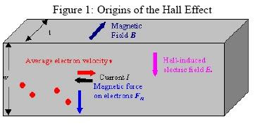
consider the situation shown in the
diagram below. In this situation, the electrons are forced downward
by the action of the magnetic field. This causes the top of the
conductor to become positive with respect to the bottom.
This causes a downward directed electric field to develop in the
conductor. This field produces an upward force on the electrons.
Equilibrium is reached when the electric force is equal to the
magnetic force. This condition is

satisfied when
The induced electric field produces a potential difference across
the conductor at a right angle to the direction of current flow.
Its magnitude is


where w is the width of the conductor. This implies that the Hall
voltage is proportional to both the electron drift velocity and the
applied field. Note also that in this instance that the Hall-induced
potential decreases from top to bottom. Suppose instead that the
charges carrying the current had been positive. In this case, the
charges average drift velocity would be in the same direction as
the current; the magnetic force on them would again force them
in the downward direction. In this case, the Hall potential then
increases from top to bottom. The sign of the Hall voltage can
therefore be used to determine the sign of the charge
carriers in a conductor.

Source ( pdf )
http://arapaho.nsuok.edu/~bradfiel/advlab/Hall/hall-effect.pdf

Friday, March 20, 2009

Hall Effect

The Hall Effect and Hall Probes

Figure 4: Diagrams of (a) a Hall bar and (b) the circuit for a Hall probe

There are a number of methods of measuring B, but the most
convenient is probably the Hall probe. Hall probes make use of the
Hall e_ect which was discovered in 1879 by Edwin Hall. When a
conducting plate (usually made of a semiconductor in practical
applications) carrying a current IH is placed in a _eld B (Fig. 4(a)),
a voltage is produced not only along the current direction, say VR
(this is the usual resistive part), but also in a ransverse direction, say
VH (this is the Hall voltage). The magnitude of VH depends on the
product of IH, the magnitude of B, and cos o, where o is the angle
between the plate normal and B. It also depends on the
thickness and type of the material. Thus


where k is a constant which we refer to as the probe constant. Notice
VH reverses when B is reversed (i.e. cos _ changes sign). Because
it is di_cult to align the Hall voltage contacts exactly opposite each
other, a part of the measured voltage is due to VR. This is the o_set
voltage V0, which may depend on the magnitude B, but does not
reverse when B is reversed. This means that V0 can be eliminated by
measuring the probe output for _B. In this experiment the probe is
powered by a constant current supply which is contained in a box.
There are two output terminals on the front of the box for the Hall
probe output voltage. There are also two output terminals on the
rear with which the Hall probe current may be checked. In order to
translate measurements of the Hall voltage into values of B, IH and
k must be recorded. The value of k is written on the power supply.
A schematic of the circuit is shown in Fig. 4(b).


Source ( pdf )
http://physics.queensu.ca/~phys250/magcirc.pdf


The Hall Effect

This subchapter introduces two important topics: The Hall effect
as an important observation in materials science and at the same
time another irrefutable proof that classical physics just can't hack
it when it comes to electrons in crystals.

- The Hall effect describes what happens to current flowing through
a conducting material - a metal, a semiconductor - if it is exposed
to a magnetic field B.

- We will look at this in classical terms; again we will encounter a
fundamental problem.


The standard geometry for doing an experiment in its most simple
form is as follows:

1.A magnetic field B is employed perpendicular to the current
direction j, as a consequence a potential difference (i.e. a voltage)
develops at right angles to both vectors.

2 In other words: A Hall voltage UHall will be measured perpendicular
to B and j.

3In yet other words: An electrical field EHall develops in y-direction

4 That is already the essence of the Hall effect.

more
http://www.tf.uni-kiel.de/matwis/amat/mw2_ge/kap_2/
backbone/r2_1_3.html